 |
 |

Beryllium Oxide Electronic Package
Specimen Preparation (Class 4 Procedures)
 |
 |
Ceramics such as alumina, beryllia (BeO) and aluminum nitride (AlN) are commonly used ceramic substrate materials for metallizing because they provide thermal conductivity and electrical resistivity.
Microstructural cross section preparation of metallized layers are difficult because of edge rounding and phase relief. In order to maintain the integrity of the metallic layers, the specimen must first be sectioned properly to avoid chipping and cracking of the ceramic substrate/metal interface. The use of SIAMAT colloidal silica also provides a chemical mechanical polishing (CMP) action, which is the most effective means for eliminating both surface and subsurface damage.
SECTIONING
Diamond Wafering blade - medium grit / low concentration
MOUNTING
Castable Mounting with Epoxy or Acrylic resins
POLISHING
| Abrasive/surface | Lubricant | Force/ sample | Speed (Head/base) |
Time | Individual Force mode |
Central Force mode |
|---|---|---|---|---|---|---|
| 45 um Diamond Lapping Film* |
POLYLUBE Diamond Extender |
5-10 lbs | 100/100 rpm | Planar |
 |
|
| 30 um Diamond Lapping Film* |
POLYLUBE Diamond Extender |
5-10 lbs | 100/100 rpm | 3 min |  |
|
| 9 um Diamond Lapping Film |
POLYLUBE Diamond Extender |
5-10 lbs | 100/100 rpm | 2 min | |
|
| 6 um DIAMAT diamond on TEXPAN polishing pad |
SIAMAT colloidal silica | 5-10 lbs | 100/100 rpm | 5 min | |
|
| 1 um DIAMAT diamond on ATLANTIS polishing pad |
SIAMAT colloidal silica | 5-10 lbs | 100/100 rpm | 5 min | |
|
| TEXPAN polishing pad | SIAMAT colloidal silica | 5 lbs | 100/100 rpm | 2 min | |
|
*Required for central polishing force. Click here for more information on central vs. individual polishing force polishing.
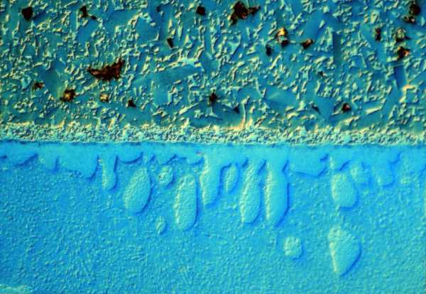 |
| BeO substrate with a nickel, copper coating, 400X (DIC) |
ETCHING
Common Etchants


CAUTION:Safety is very important when etching. Be sure to wear the appropriate protective clothing and observe all WARNINGS on chemical manufacuters SDS (Safety Data Sheets). Also review the COMMENTS and CONDITIONS Section for each etchant.
PACE TECHNOLOGIES CONTACT
PACE Technologies
3601 E. 34th St.
Tucson, Arizona 85713
+1-520-882-6598
FAX +1-520-882-6599
email: pace@metallographic.com
https://www.metallographic.com